Introduction
What is the LL-RLP-20 or LL-RXR-27 Module?
The LL-RLP-20 or LL-RXR-27 Module is a highly-integrated, low-power, bi-directional radio transceiver module. The modules are optimized for use either in the 915-MHz ISM frequency band or the 868-MHz ETSI frequency band. The modules use a Frequency Modulated Chirp (Semtech's LoRaTM modulation) to maximize range while minimizing power consumption and interference.
The LL-RLP-20 and LL-RXR-27 are essentially identical, with the exception that the LL-RXR-27 includes an onboard power amplifier in the transmit path and a low-noise amplifier in the receive path. The maximum transmit power of the RXR-27 therefore exceeds that of the RLP-20 by approximately 6 dB.
Key Features
LL-RLP-20
- Receiver sensitivity: -140 dBm
- Transmit power: 60 mW / 17.5 dBm
- TX Peak Current: 122 mA
- RX Peak Current: 10 mA
- Sleep current: less than 1 uA (regulated/direct), less than 10 uA (unregulated)
LL-RXR-27
- Receiver sensitivity: -137 dBm
- Transmit power: 250 mW / 24 dBm
- Tx Peak Current: 480 mA
- Rx Peak Current: 40 mA
- Sleep current: less than 1 uA (regulated/direct), less than 10 uA (unregulated)
Hardware Specifications
LL-RLP-20 Hardware Specifications
The following table presents the hardware specifications of the LL-RLP-20 module.
|
Frequency bands |
902-to-928 MHz ISM (US); 868 MHz ETSI (EU) |
|
On-air data rate |
183 bps to 1 kbps |
|
Output power |
Programmable: 18 dBm to 4 dBm in 0.6 dB steps |
|
Supply voltage |
3.5 V to 5.5 V |
|
VCC |
3.3 V (if using onboard regulator) 2.7 – 3.6 V (if supplying regulated voltage) |
|
Onboard regulator |
VIN = 3.5 – 5.5 V VOUT = 3.3 V Max current = 250 mA Iq = 7.9 μA PSRR = 85 dB at 10 Hz, 70 dB at 1 kHz, 40 dB at 100 kHz |
|
I/O voltage |
3.3 V typical (if using onboard regulator) VIH: min = 0.8 x VCC; max = VCC + 0.3 VIL: min = -0.3; max = 0.2 x VCC |
|
Tx peak current |
122 mA |
|
Rx current |
10 mA |
|
Sleep current |
< 1 μA (regulated/direct) < 10 μA (unregulated) |
|
Dimensions |
24.5 mm x 29 mm; 2.66 mm thick with RF shield |
|
Operating temp. |
-20 to 70 C |
|
UART baud rate |
115200 8n1 |
LL-RXR-27 Hardware Specifications
The following table presents the hardware specifications of the LL-RXR-27 module.
|
Frequency bands |
902-to-928 MHz ISM (US); 868 MHz ETSI (EU) |
|
On-air data rate |
183 bps to 1 kbps |
|
Output power |
Programmable: 26 dBm to 12 dBm in 0.6 dB steps |
|
Supply voltage |
3.5 V to 5.5 V |
|
VCC |
3.3 V |
|
Onboard regulator |
VIN = 3.5 – 5.5 V VOUT = 3.3 V Max current = 150 mA Iq = 1 μA PSRR = 50 dB |
|
I/O voltage |
3.3 V typical VIH: min = 0.8 x VCC; max = VCC + 0.3 VIL: min = -0.3; max = 0.2 x VCC |
|
Tx peak current |
480 mA |
|
Rx current |
40 mA |
|
Sleep current |
< 1 μA (regulated/direct) < 10 μA (unregulated) |
|
Dimensions |
24.5 mm x 29 mm; 2.66 mm thick with RF shield |
|
Operating temp. |
-20 to 70 C |
|
UART baud rate |
115200 8n1 |
Applicable EU Frequency Bands
The following table presents the applicable frequency bands according to ERC Recommendation 70-03.
|
Band |
Edge Frequencies (MHz) |
TX Power (dBm) |
Duty Cycle |
Bandwidth (kHz) |
|
|
g |
865.0 |
868.0 |
+6.2 / 100kHz |
1% or LBT + AFA |
3000 |
|
g1 |
868.0 |
868.6 |
+14 |
1% or LBT + AFA |
600 |
|
g2 |
868.7 |
869.2 |
+14 |
0.1% or LBT + AFA |
500 |
|
g3 |
869.4 |
869.65 |
+27 |
10% or LBT + AFA |
250 |
|
g4 |
869.7 |
870 |
+14 |
1% or LBT + AFA |
300 |
|
g4 |
869.7 |
870 |
+7 |
No requirement |
300 |
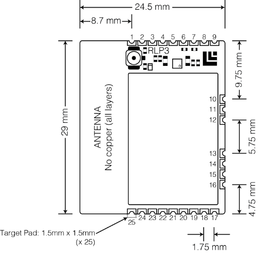
Footprint and Pinout
The LL-RLP-20 and the LL-RXR-27 share the same footprint and pinout.
Footprint
The following figure depicts the footprint of the LL-RLP-20 and/or LL-RXR-27 module.
Pinout
|
Pin #1 |
Name |
Type |
Description |
|
1 |
GND |
Ground |
|
|
2 |
ANT2,3 |
RF I/O |
RF path if not using U.FL connector |
|
3 |
VBAT |
Input voltage |
Optional unregulated supply voltage (3.5 to 5.5 V) |
|
4 |
LDO_OUT4 |
Output voltage |
Power digital (3.3 V) |
|
5 |
VCC |
Input voltage |
Regulated supply voltage (2.5 to 3.3 V) |
|
6 |
N/C |
Float |
|
|
7 |
nRESET |
I |
External reset pin, active low |
|
8 |
IO0 |
O |
Status message indicator |
|
9 |
GND |
Ground |
|
|
10 |
N/C |
Float |
|
|
11 |
N/C |
Float |
|
|
12 |
N/C |
Float |
|
|
13 |
N/C |
Float |
|
|
14 |
N/C5 |
Float |
|
|
15 |
N/C |
Float |
|
|
16 |
N/C |
Float |
|
|
17 |
nBOOT |
I |
N/C = Boot normally, GND = Bootloader |
|
18 |
N/C |
Float |
|
|
19 |
N/C |
Float |
|
|
20 |
N/C |
Float |
|
|
21 |
N/C |
Float |
|
|
22 |
N/C |
Float |
|
|
23 |
RXIN6 |
I |
UART interface: module RX |
|
24 |
TXOUT6 |
O |
UART interface: module TX |
|
25 |
GND |
Ground |
1All not-connected pins should be floated.
2RF connection is via U.FL connector on upper left side of the module or pin 2.
3RF output is 50 Ohms, DC blocking capacitor not required.
4If using VBAT, must tie LDO_OUT to VCC.
5If Pin 14 is floating or high, UART baud rate is 115200. If Pin 14 is grounded or low, UART baud rate is 9600.
6Default UART baud rate is 115200 8n1.
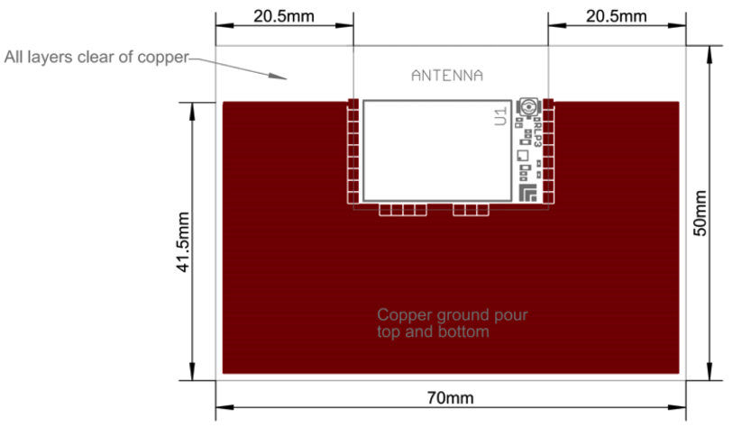
Carrier Board Layout Requirements
Because the LL-RLP-20 and LL-RXR-27 and their associated antennas have been certified by the FCC and Industry Canada (IC) as a Modular Radios, the end-user is authorized to integrate these modules into end-products, and is solely responsible for the Unintentional Emissions levels produced by the end-product.
In order to preserve the Modular Radio certifications, the integrator of the module must abide by the PCB layout recommendations in the following paragraphs. Any divergence from these recommendations will invalidate the Modular Radio certifications and require the integrator to re-certify the module and/or end product.
The following applies to both the LL-RLP-20 and the LL-RXR-27.
The module must be used with one of the approved antennas:
- 1/2-wave center-fed dipole antennas tuned for 915 MHz with a maximum gain of 1.9 dBi or less, such as ANT-916-CW-HWR-SMA.
- Integrated trace antenna.
Trace Antenna Design
EAGLE library
Link-Labs-Modules_Public.lbrSTEP files
LL-RLP-20 module with trace antenna
STEP file with antennaLL-RLP-20 module without trace antenna
STEP file without antennaReflow Guidelines
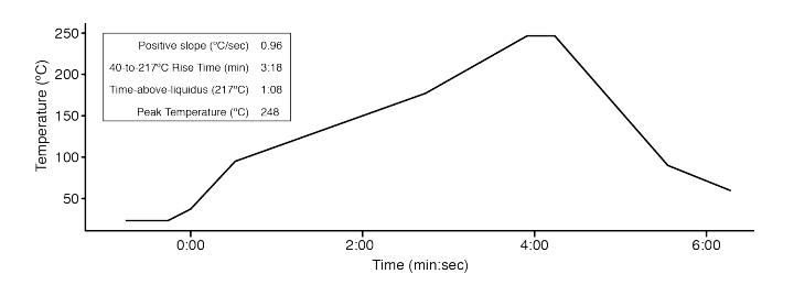
This article provides reflow guidelines for surface mounting the LL-RLP-20 or LL-RXR-27 module to a carrier board using lead-free solder.
Temperature-time profile
None of the components on the LL-RLP-20 or LL-RXR-27 are particularly sensitive with regards to peak reflow temperatures. Printed circuit board manufacturers may therefore typically rely on solder paste guidelines to construct a reflow profile.
The following parameters should be used for reflow with tin-silver-copper (SAC alloy) solder:
- Straight ramp profile with ramp rate of 0.8 to 1.5 degrees Celsius per second
- Peak temperature between 240 and 255 degrees Celsius
- TAL (time above liquidus) of 35 to 80 seconds
Example profile
The following temperature-time profile is used to surface mount the LL-RLP-20 or LL-RXR-27 to its Evaluation Board.
Regulatory Compliance Information
U.S./Canada Regulatory Compliance Information
To satisfy FCC RF exposure requirements for mobile and base station transmission devices, a separation distance of 20 cm or more should be maintained between the antenna of this device and persons during operation. To ensure compliance, operation at closer than this distance is not recommended. The antenna(s) used for this transmitter must not be co-located or operating in conjunction with any other antenna or transmitter.
U.S./Canada OEM Labeling Requirements for End-Product
The module is labeled with its own FCC ID and IC Certification Number. The FCC ID and IC Certification Numbers are not visible when the module is installed inside another device. As such the end device into which the module is installed must display a label referring to the enclosed module. The final end product must be labeled in a visible area with the following:
LL-RLP-20
"Contains Transmitter Module FCC ID: 2ACT6LLRLP20" and "Contains Transmitter Module IC: 12201A-LLRLP20"
or
"Contains FCC ID: 2ACT6LLRLP20" and "Contains IC: 12201A-LLRLP20"
LL-RXR-27
"Contains Transmitter Module FCC ID: 2ACT6LLRXR27" and "Contains Transmitter Module IC: 12201A-LLRXR27"
or
"Contains FCC ID: 2ACT6LLRXR27" and "Contains IC: 12201A-LLRXR27"
The OEM of the module must only use approved antenna(s) listed above, which have been certified with the module.
OEM End-Product User Manual Statements
The OEM integrator should not provide information to the end user regarding how to install or remove this RF module or change RF related parameters in the user manual of the end product.
Other user manual statements may apply.
Federal Communication Commission Interference Statement
This equipment has been tested and found to comply with the limits for a Class B digital device, pursuant to Part 15 of the FCC Rules. These limits are designed to provide reasonable protection against harmful interference in a residential installation. This equipment generates uses and can radiate radio frequency energy and, if not installed and used in accordance with the instructions, may cause harmful interference to radio communications. However, there is no guarantee that interference will not occur in a particular installation. If this equipment does cause harmful interference to radio or television reception, which can be determined by turning the equipment off and on, the user is encouraged to try to correct the interference by one of the following measures:
- Reorient or relocate the receiving antenna.
- Increase the separation between the equipment and receiver.
- Connect the equipment into an outlet on a circuit different from that to which the receiver is connected.
- Consult the dealer or an experienced radio/TV technician for help.
This device complies with Part 15 of the FCC Rules. Operation is subject to the following two conditions: (1) This device may not cause harmful interference, and (2) this device must accept any interference received, including interference that may cause undesired operation.
FCC CAUTION: Any changes or modifications not expressly approved by the party responsible for compliance could void the user's authority to operate this equipment.
Conformité aux normes FCC Cet équipement a été testé et trouvé conforme aux limites pour un dispositif numérique de classe B, conformément à la Partie 15 des règlements de la FCC. Ces limites sont conçues pour fournir une protection raisonnable contre les interférences nuisibles dans une installation résidentielle.
Cet équipement génère, utilise et peut émettre des fréquences radio et, s’il n’est pas installé et utilisé conformément ment aux instructions du fabricant, peut causer des interferences nuisibles aux communications radio.
Rien ne garantit cependant que l’interférence ne se produira pas dans une installation particulière. Si cet équipement provoque des interférences nuisibles à la réception radio ou de télévision, qui peut être déterminé en comparant et en l’éteignant, l’utilisateur est encouragé à essayer de corriger les interférence par une ou plusieurs des mesures suivantes:
- Réorienter ou déplacer l’antenne de réception.
- Augmenter la distance entre l’équipement et le récepteur.
- Branchez l’appareil dans une prise sur un circuit différent de celui auquel le récepteur est connecté.
- Consultez votre revendeur ou un technicien radio / TV pour assistance.Avertissement
Les changements ou modififications à cet appareil sans expressément approuvée par la partie responsable de conformité pourraient annuler l’autorité de l’utilisateur de faire fonctionner cet équipement.
Industry Canada Statements
This device complies with Industry Canada license-exempt RSS standard(s). Operation is subject to the following two conditions: (1) this device may not cause interference, and (2) this device must accept any interference, including interference that may cause undesired operation of the device.
This device complies with RSS-210 of the Industry Canada Rules. Operation is subject to the following two conditions: (1) this device may not cause interference, and (2) this device must accept any interference, including interference that may cause undesired operation of the device.
To reduce potential radio interference to other users, the antenna type and its gain should be so chosen that the equivalent isotropically radiated power (e.i.r.p.) is not more than that permitted for successful communication.
This device has been designed to operate with the antennas listed in the filing, and having a maximum gain of 1.9 dBi. Antennas not included in this list or having a gain greater than 1.9 dBi are strictly prohibited for use with this device. The required antenna impedance is 50 ohms.
Cet appareil est conforme avec Industrie Canada exempt de licence Rss standard(s). Son fonctionnement est soumis aux deux conditions suivantes : (1) cet appareil ne peut causer d’interférences, et (2) cet appareil doit accepter toute interférence, y compris des interférences qui peuvent provoquer un fonctionnement indésirable du périphérique.
Ce dispositif est conforme à la norme CNR-210 d’Industrie Canada applicable aux appareils radio exempts de licence. Son fonctionnement est sujet aux deux conditions suivantes: (1) le dispositif ne doit pas produire de brouillage préjudiciable, et (2) ce dispositif doit accepter tout brouillage reçu, y compris un brouillage susceptible de provoquer un fonctionnement indésirable.
Pour réduire le risque d’interférence aux autres utilisateurs, le type d’antenne et son gain doivent être choisies de façon que la puissance isotrope rayonnée équivalente (e.i.r.p) ne dépasse pas celle admise pour une communication réussie.
Cet appareil a été conçu pour fonctionner avec les antennes énumérées ci-dessous, et ayant un gain maximum de 6,0 dB. Antennes pas inclus dans cette liste ou ayant un gain supérieur à 6,0 dB sont strictement interdites pour une utilisation avec cet appareil. L’impédance d’antenne requise est de 50 ohms.
ETSI Compliance Information
The use of radio frequencies is limited by national regulations. The radio module has been designed to comply with the European Union’s R&TTE (Radio & Telecommunications Terminal Equipment) directive 1999/5/EC and can be used free of charge within the European Union. Nevertheless, restrictions in terms of maximum allowed RF power or duty cycle may apply.
The radio module has been designed to be embedded into other products (referred as ”final products”). According to the R&TTE directive, the declaration of compliance with essential requirements of the R&TTE directive is within the responsibility of the manufacturer of the final product. A declaration of conformity for the radio module is available from Link Labs, LLC on request.
The applicable regulation requirements are subject to change. Link Labs does not take any responsibility for the correctness and accuracy of the aforementioned information. National laws and regulations, as well as their interpretation can vary with the country. In case of uncertainty, it is recommended to contact either Link Labs’ accredited Test Center or to consult the local authorities of the relevant countries.
Important Notice
Disclaimer
Link Labs, Inc. (hereafter referred to as ”Link Labs”), reserves the right to make corrections, enhancements, improvements and other changes to its products and services. Buyers should obtain the latest relevant information before placing orders and should verify that such information is current and complete. All products (also referred to herein as ”components”) are sold subject to Link Labs terms and conditions of sale supplied at the time of order acknowledgment.
Link Labs warrants performance of its components to the specifications applicable at the time of sale, in accordance with the warranty in Link Labs’ terms and conditions of sale. Testing and other quality control techniques are used to the extent Link Labs deems necessary to support this warranty. Except where mandated by applicable law, testing of all parameters of each component is not necessarily performed.
Link Labs assumes no liability for applications assistance or the design of Buyers’ products. Buyers are responsible for their products and applications using Link Labs components. To minimize the risks associated with Buyers products and applications, Buyers should provide adequate design and operating safeguards.
Link Labs does not warrant or represent that any license, either express or implied, is granted under any patent right, copyright, mask work right, or other intellectual property right relating to any combination, machine, or process in which Link Labs components or services are used. Information published by Link Labs regarding third-party products or services does not constitute a license to use such products or services or a warranty or endorsement thereof. Use of such information may require a license from a third party under the patents or other intellectual property of the third party, or a license from Link Labs under the patents or other intellectual property of Link Labs.
Reproduction of significant portions of Link Labs information in Buyers’ data books or data sheets is permissible only if reproduction is without alteration and is accompanied by all associated warranties, conditions, limitations, and notices. Link Labs is not responsible or liable for such altered documentation. Information of third parties may be subject to additional restrictions.
Resale of Link Labs components or services with statements different from or beyond the parameters stated by Link Labs for that component or service voids all express and any implied warranties for the associated Link Labs component or service and is an unfair and deceptive business practice. Link Labs is not responsible or liable for any such statements.
Buyer acknowledges and agrees that it is solely responsible for compliance with all legal, regulatory and safety- related requirements concerning its products, and any use of Link Labs components in its applications, notwithstanding any applications-related information or support that may be provided by Link Labs. Buyer represents and agrees that it has all the necessary expertise to create and implement safeguards which anticipate dangerous consequences of failures, monitor failures and their consequences, lessen the likelihood of failures that might cause harm and take appropriate remedial actions. Buyer will fully indemnify Link Labs and its representatives against any damages arising out of the use of any Link Labs components in safety-critical applications.
In some cases, Link Labs components may be promoted specifically to facilitate safety-related applications. With such components, Link Labs’ goal is to help enable customers to design and create their own end-product solutions that meet applicable functional safety standards and requirements. Nonetheless, such components are subject to these terms.
No Link Labs components are authorized for use in FDA Class III (or similar life-critical medical equipment) unless authorized officers of the parties have executed a special agreement specifically governing such use.
Only those Link Labs components which Link Labs has specifically designated as military grade are designed and intended for use in military/aerospace applications or environments. Buyer acknowledges and agrees that any military or aerospace use of Link Labs components which have not been so designated is solely at the Buyer’s risk, and that Buyer is solely responsible for compliance with all legal and regulatory requirements in connection with such use.