Hardware Specifications
| RF Specifications | Value |
|---|---|
| Maximum Transmit Power | 23 dBm |
| Receive Sensitivity | -103 dBm |
| Technology | LTE CAT-M1, 3GPP Release 13 Compliant |
| Modulation | QPSK, 16QAM |
| Supported LTE Bands* | B4 (AWS1700)/ B13 (700) |
| Security | Verizon VPN |
| Downlink Data Rate | 300 kbps DL |
| Uplink Data Rate | 375 kbps UL in HD-FDD, and 1 Mbps in FD-DD |
| Regulatory | Value |
| Regulatory Approvals | FCC (2AAGMVZM20Q), IC |
| Carrier Pre-Certification | Verizon |
| Market | North America |
| Electrical Specifications | Value |
| Supply Voltage | 3.1-4.5 VDC |
| Peak Transmit Current | 560 mA |
| Receive Current | 330 mA |
| Idle Current/Sleep Mode | 10 uA |
| Serial Data Interface | UART |
| Chipset | Link Labs / Sequans |
| Physical Specifications | Value |
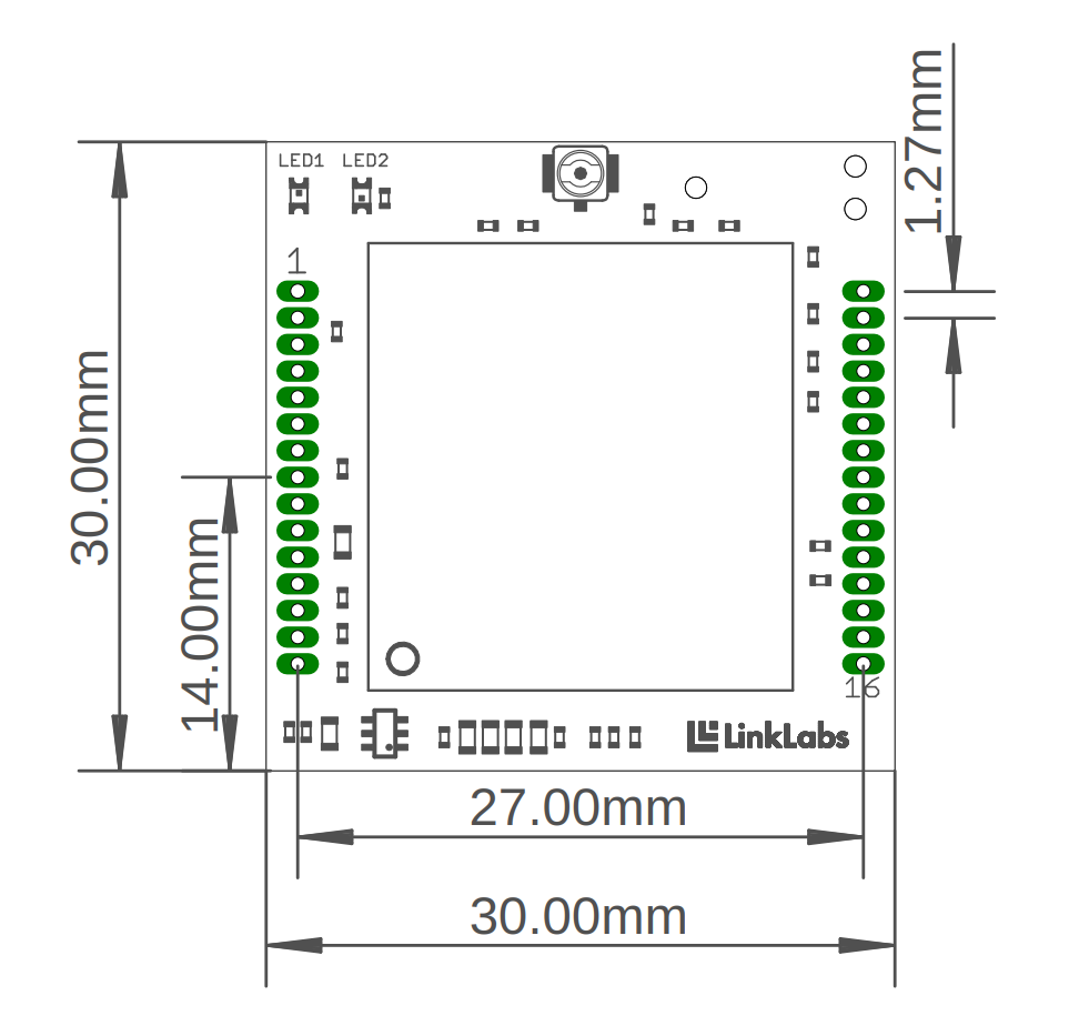
| Dimensions | 30 mm x 30 mm |
| Operating Temperature (RF Compliant) | -30 C to 60 C (Ambient Temperature) |
| Storage/Operating Temperature | -40 C to 85 C (Board) |
| Operating Humidity | 10% to 85% (Non-condensing) |
Footprint and Pinout
Footprint

Pinout
|
Pin # |
Name |
Type |
Description |
|
1 |
N/C |
No Contact |
Float |
|
2 |
GND |
Ground |
Ground |
|
3 |
PROG_RESET1 |
SWD Prog |
External reset pin, active low |
|
4 |
PROG_SWCLK1 |
SWD Prog |
Module SWCLK programming |
|
5 |
PROG_SWDIO1 |
SWD Prog |
Module SWDIO programming |
|
6 |
MOD_CTS |
I |
UART interface: Module CTS |
|
7 |
MOD_RTS |
O |
UART interface: Module RTS |
|
8 |
MOD_RXIN |
I |
UART interface: Module RX |
|
9 |
MOD_TXOUT |
O |
UART interface: Module TX |
|
10 |
GND |
Ground |
Ground |
|
11 |
MOD_TX_DEBUG2 |
O |
UART interface: Module Debug TX |
|
12 |
MOD_RX_DEBUG2 |
I |
UART interface: Module Debug RX |
|
13 |
MOD_WAKE_STATUS/GPIO |
O |
Module Status Indicator |
|
14 |
+1V8_IO
|
Output voltage |
Power digital IO (1.8V) |
|
15 |
V+
|
Input voltage |
Supply Voltage (3.1-4.5V) |
|
16 |
N/C |
No Contact |
Float |
|
17 |
GND |
Ground |
Ground |
|
18 |
SQN_UART1_RTS3 |
O |
UART Interface: SQN_1 Debug RTS |
|
19 |
SQN_UART1_CTS3 |
I |
UART interface: SQN_1 Debug CTS |
|
20 |
SQN_UART1_RX3 |
I |
UART interface: SQN_1 Debug RX |
|
21 |
SQN_UART1_TX3 |
O |
UART interface: SQN_1 Debug TX |
|
22 |
nBOOT |
I |
N/C = Boot Normally, GND = Bootloader |
|
23 |
MOD_HOST_NOTIFY/IO0 |
O |
Module Notify Host Indicator |
|
24 |
MOD_WAKE_REQUEST/IO1 |
I |
Module Wake Request from Host |
|
25 |
GND |
Ground |
Ground |
|
26 |
SQN_UART2_CTS4 |
I |
UART interface: SQN_2 Debug CTS |
|
27 |
SQN_UART2_RTS4 |
O |
UART interface: SQN_2 Debug RTS |
|
28 |
SQN_UART2_TX4 |
O |
UART interface: SQN_2 Debug TX |
|
29 |
3V3_IO1 |
Output Voltage |
Power Digital IO (3.3V) |
|
30 |
SQN_UART2_RX4 |
I |
UART interface: SQN_2 Debug RX |
1Module programming pins. Module comes pre-programmed with latest FW and bootloader. Float if not used.
2Debug UART for module, Baud: 921600 (development only)
3Debug UART1 for SQN chipset. Baud: 115200 (development only)
4Debug UART2 for SQN chipset. Baud: 921600 (development only)
- All not connected pins should be floated.
- Default module UART baud rate is 115200 8n1 w/ HW flow control
- 1.8V IO used for logic level translation on SQN UART debug (development only). DO NOT use as 1.8V power source.
- 3.3V IO used for logic level translation for module UART. Low output current, NOT recommended for 3.3V power source other than lower current consumption level translation. Connect to programmer VCC if programming module.
- V+ lower than 3.5V will cause host logic level to be lower than 3.3V.
- RF connection is via U.FL connector.
Pin profile

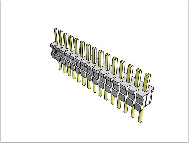
The board uses 2x, 15 pin, TMS-115-02-F-S, connectors for mating to the host board.
3D Design Files
Included in download:
- LL-LTE-M-VZN-SE ACIS.SAT
- LL-LTE-M-VZN-SE AP214.STEP
- LL-LTE-M-VZN-SE AP214 STEP assembly.STEP
- LL-LTE-M-VZN-SE OBJ Mesh.OBJ
- LL-LTE-M-VZN-SE Parasolid.X_T
- LL-LTE-M-VZN-SE STL part.STL
